RPI4 + 7C81 + DMB4250-8B BreakOut Board
- brianvg
- Offline
- New Member
-

Less
More
- Posts: 6
- Thank you received: 0
28 Feb 2021 13:10 #200405
by brianvg
RPI4 + 7C81 + DMB4250-8B BreakOut Board was created by brianvg
Hi,
I am trying to use PNC conf to get to a working configuration for the Mesa 7C81. My machine uses a breakout board from DMM, the DMB4250-8B BreakOut Board. This is sort of similar to the chinese BOB that seem to be widely used, but does not, as far as I can tell, use the same pinout. When I read the configuration currently loaded on the 7C81:
I have been consulting the thread here , which has a lot of useful information, but I am not sure how to make that last step of mapping the pins i need to their respective outputs to connect to my breakout board. I have attached a screenshot of the pinout of the breakout board. Since this is "non-standard" pinout for the DB25, is it required that I create a custom bitstream for the 7c81? It would surprise me if all pin functionalities were multiplexed to all pins on the FPGA. I presume only the "primary" pin function and GPIO uses are multiplexed. As you can see, my pinout is not compatible with what is currently configured on the 7c81.
I could also imagine using some sort of interposing board that crosses all the required pins from one location to another, but I don't particularly relish the thought of doing that.
I had the machine working with a simple parallel port, but it was too slow and I need to add an additional independent motor and homing switch, as the machine has a gantry, and I could never get proper alignment with the two gantry motors when they run from the same step/dir source.
Could someone give me some guidance? I am a beginner with Linux CNC, but I have some experience with FPGA's.
Thanks,
Brian
I am trying to use PNC conf to get to a working configuration for the Mesa 7C81. My machine uses a breakout board from DMM, the DMB4250-8B BreakOut Board. This is sort of similar to the chinese BOB that seem to be widely used, but does not, as far as I can tell, use the same pinout. When I read the configuration currently loaded on the 7C81:
halcmd: loadrt hostmot2
Note: Using POSIX realtime
hm2: loading Mesa HostMot2 driver version 0.15
halcmd: loadrt hm2_rpspi
hm2/hm2_7c81.0: Low Level init 0.15
hm2/hm2_7c81.0: Smart Serial Firmware Version 43
hm2/hm2_7c81.0: 57 I/O Pins used:
hm2/hm2_7c81.0:     IO Pin 000 (P1-01): PWMGen #0, pin Out0 (PWM or Up) (Output)
hm2/hm2_7c81.0:     IO Pin 001 (P1-02): IOPort
hm2/hm2_7c81.0:     IO Pin 002 (P1-03): StepGen #0, pin Step (Output)
hm2/hm2_7c81.0:     IO Pin 003 (P1-04): IOPort
hm2/hm2_7c81.0:     IO Pin 004 (P1-05): StepGen #0, pin Direction (Output)
hm2/hm2_7c81.0:     IO Pin 005 (P1-06): IOPort
hm2/hm2_7c81.0:     IO Pin 006 (P1-07): StepGen #1, pin Step (Output)
hm2/hm2_7c81.0:     IO Pin 007 (P1-08): IOPort
hm2/hm2_7c81.0:     IO Pin 008 (P1-09): StepGen #1, pin Direction (Output)
hm2/hm2_7c81.0:     IO Pin 009 (P1-11): StepGen #2, pin Step (Output)
hm2/hm2_7c81.0:     IO Pin 010 (P1-13): StepGen #2, pin Direction (Output)
hm2/hm2_7c81.0:     IO Pin 011 (P1-15): StepGen #3, pin Step (Output)
hm2/hm2_7c81.0:     IO Pin 012 (P1-17): StepGen #3, pin Direction (Output)
hm2/hm2_7c81.0:     IO Pin 013 (P1-19): IOPort
hm2/hm2_7c81.0:     IO Pin 014 (P1-21): Encoder #0, pin A (Input)
hm2/hm2_7c81.0:     IO Pin 015 (P1-23): Encoder #0, pin B (Input)
hm2/hm2_7c81.0:     IO Pin 016 (P1-25): Encoder #0, pin Index (Input)
hm2/hm2_7c81.0:     IO Pin 017 (J5-TX0): IOPort
hm2/hm2_7c81.0:     IO Pin 018 (J6-TX1): IOPort
hm2/hm2_7c81.0:     IO Pin 019 (P2-01): PWMGen #1, pin Out0 (PWM or Up) (Output)
hm2/hm2_7c81.0:     IO Pin 020 (P2-02): IOPort
hm2/hm2_7c81.0:     IO Pin 021 (P2-03): StepGen #4, pin Step (Output)
hm2/hm2_7c81.0:     IO Pin 022 (P2-04): IOPort
hm2/hm2_7c81.0:     IO Pin 023 (P2-05): StepGen #4, pin Direction (Output)
hm2/hm2_7c81.0:     IO Pin 024 (P2-06): IOPort
hm2/hm2_7c81.0:     IO Pin 025 (P2-07): StepGen #5, pin Step (Output)
hm2/hm2_7c81.0:     IO Pin 026 (P2-08): IOPort
hm2/hm2_7c81.0:     IO Pin 027 (P2-09): StepGen #5, pin Direction (Output)
hm2/hm2_7c81.0:     IO Pin 028 (P2-11): StepGen #6, pin Step (Output)
hm2/hm2_7c81.0:     IO Pin 029 (P2-13): StepGen #6, pin Direction (Output)
hm2/hm2_7c81.0:     IO Pin 030 (P2-15): IOPort
hm2/hm2_7c81.0:     IO Pin 031 (P2-17): IOPort
hm2/hm2_7c81.0:     IO Pin 032 (P2-19): IOPort
hm2/hm2_7c81.0:     IO Pin 033 (P2-21): IOPort
hm2/hm2_7c81.0:     IO Pin 034 (P2-23): IOPort
hm2/hm2_7c81.0:     IO Pin 035 (P2-25): IOPort
hm2/hm2_7c81.0:     IO Pin 036 (J5-TXEN0): IOPort
hm2/hm2_7c81.0:     IO Pin 037 (J6-TXEN1): IOPort
hm2/hm2_7c81.0:     IO Pin 038 (P7-01): PWMGen #2, pin Out0 (PWM or Up) (Output)
hm2/hm2_7c81.0:     IO Pin 039 (P7-02): IOPort
hm2/hm2_7c81.0:     IO Pin 040 (P7-03): StepGen #7, pin Step (Output)
hm2/hm2_7c81.0:     IO Pin 041 (P7-04): IOPort
hm2/hm2_7c81.0:     IO Pin 042 (P7-05): StepGen #7, pin Direction (Output)
hm2/hm2_7c81.0:     IO Pin 043 (P7-06): IOPort
hm2/hm2_7c81.0:     IO Pin 044 (P7-07): StepGen #8, pin Step (Output)
hm2/hm2_7c81.0:     IO Pin 045 (P7-08): IOPort
hm2/hm2_7c81.0:     IO Pin 046 (P7-09): StepGen #8, pin Direction (Output)
hm2/hm2_7c81.0:     IO Pin 047 (P7-11): StepGen #9, pin Step (Output)
hm2/hm2_7c81.0:     IO Pin 048 (P7-13): StepGen #9, pin Direction (Output)
hm2/hm2_7c81.0:     IO Pin 049 (P7-15): IOPort
hm2/hm2_7c81.0:     IO Pin 050 (P7-17): IOPort
hm2/hm2_7c81.0:     IO Pin 051 (P7-19): IOPort
hm2/hm2_7c81.0:     IO Pin 052 (P7-21): IOPort
hm2/hm2_7c81.0:     IO Pin 053 (P7-23): IOPort
hm2/hm2_7c81.0:     IO Pin 054 (P7-25): IOPort
hm2/hm2_7c81.0:     IO Pin 055 (P5-RX0): IOPort
hm2/hm2_7c81.0:     IO Pin 056 (P6-RX1): IOPort
hm2/hm2_7c81.0: registered
I have been consulting the thread here , which has a lot of useful information, but I am not sure how to make that last step of mapping the pins i need to their respective outputs to connect to my breakout board. I have attached a screenshot of the pinout of the breakout board. Since this is "non-standard" pinout for the DB25, is it required that I create a custom bitstream for the 7c81? It would surprise me if all pin functionalities were multiplexed to all pins on the FPGA. I presume only the "primary" pin function and GPIO uses are multiplexed. As you can see, my pinout is not compatible with what is currently configured on the 7c81.
I could also imagine using some sort of interposing board that crosses all the required pins from one location to another, but I don't particularly relish the thought of doing that.
I had the machine working with a simple parallel port, but it was too slow and I need to add an additional independent motor and homing switch, as the machine has a gantry, and I could never get proper alignment with the two gantry motors when they run from the same step/dir source.
Could someone give me some guidance? I am a beginner with Linux CNC, but I have some experience with FPGA's.
Thanks,
Brian
Please Log in or Create an account to join the conversation.
- PCW
-

- Offline
- Moderator
-

Less
More
- Posts: 17916
- Thank you received: 5245
28 Feb 2021 15:31 #200424
by PCW
Replied by PCW on topic RPI4 + 7C81 + DMB4250-8B BreakOut Board
The DMM BOB is pretty standard but I had not made a 7C81 config for it yet, but here it is:
Please Log in or Create an account to join the conversation.
- brianvg
- Offline
- New Member
-
Less
More
- Posts: 6
- Thank you received: 0
28 Feb 2021 16:33 #200435
by brianvg
Replied by brianvg on topic RPI4 + 7C81 + DMB4250-8B BreakOut Board
Thanks PCW! I was able to write your bitfile to the EEPROM .
However, the reload operation does not seem to be working:
This runs ok, but then when I run
The results look the same as with the default configuration. Do I need to do an actual power cycle? Maybe running the --reload command is reloading the contents of the flash starting from address 0x0?
FInally, with the new pinout, will it still be possible to use pncconf, or will I need to go in and manually set the pin numbers? I.E. run through the configuration process as though it was using the 2x chinese BOB, and then manually change all of the pin assignments?
Thanks for your help,
Brian
However, the reload operation does not seem to be working:
mesaflash --device 7C81 --spi --addr /dev/spidev0.0 --reload
unable to set bpw32, fallback to bpw8
Waiting for FPGA configuration...OK
This runs ok, but then when I run
mesaflash --device 7C81 --spi --addr /dev/spidev0.0 --readhmidThe results look the same as with the default configuration. Do I need to do an actual power cycle? Maybe running the --reload command is reloading the contents of the flash starting from address 0x0?
FInally, with the new pinout, will it still be possible to use pncconf, or will I need to go in and manually set the pin numbers? I.E. run through the configuration process as though it was using the 2x chinese BOB, and then manually change all of the pin assignments?
Thanks for your help,
Brian
Please Log in or Create an account to join the conversation.
- PCW
-
- Offline
- Moderator
-
Less
More
- Posts: 17916
- Thank you received: 5245
28 Feb 2021 16:56 - 28 Feb 2021 16:58 #200437
by PCW
Replied by PCW on topic RPI4 + 7C81 + DMB4250-8B BreakOut Board
The DMM pinout is very similar to the default 5ABOB, the main difference being that the DMMBOB has dir,step,dir,step instead of step/dir,step
You should be able to use pncconf with the possible exception of some GPIO setup
(and driver/card name)
You should be able to use pncconf with the possible exception of some GPIO setup
(and driver/card name)
Last edit: 28 Feb 2021 16:58 by PCW.
Please Log in or Create an account to join the conversation.
- brianvg
- Offline
- New Member
-
Less
More
- Posts: 6
- Thank you received: 0
28 Feb 2021 17:21 #200440
by brianvg
Replied by brianvg on topic RPI4 + 7C81 + DMB4250-8B BreakOut Board
Ahh, yes, I see. I was not looking carefully. Indeed the output is different, with just the direction and step swapped after loading the new firmware. But is that really the only difference between the 5ABOB and the DMM breakout?
For instance, in the new pinout:
I note that there are also unused pins between the step and direction pins. Is that really the case? In my read of the DMM schematics, the step and direction pins are on neighboring pins? Maybe I am missing something...
E.G. it should look something like this:
Thats my read of the schematic, operating on the assumption that P1-xx refers to the pins of the db25 connector? I may be misunderstanding something though...
Best,
Brian
For instance, in the new pinout:
halrun
halcmd: loadrt hostmot2
Note: Using POSIX realtime
hm2: loading Mesa HostMot2 driver version 0.15
halcmd:  loadrt hm2_rpspi
hm2/hm2_7c81.0: Low Level init 0.15
hm2/hm2_7c81.0: Smart Serial Firmware Version 43
hm2/hm2_7c81.0: 57 I/O Pins used:
hm2/hm2_7c81.0:     IO Pin 000 (P1-01): PWMGen #0, pin Out0 (PWM or Up) (Output)
hm2/hm2_7c81.0:     IO Pin 001 (P1-02): IOPort
hm2/hm2_7c81.0:     IO Pin 002 (P1-03): StepGen #0, pin Direction (Output)
hm2/hm2_7c81.0:     IO Pin 003 (P1-04): IOPort
hm2/hm2_7c81.0:     IO Pin 004 (P1-05): StepGen #0, pin Step (Output)
hm2/hm2_7c81.0:     IO Pin 005 (P1-06): IOPort
hm2/hm2_7c81.0:     IO Pin 006 (P1-07): StepGen #1, pin Direction (Output)
hm2/hm2_7c81.0:     IO Pin 007 (P1-08): IOPort
hm2/hm2_7c81.0:     IO Pin 008 (P1-09): StepGen #1, pin Step (Output)
hm2/hm2_7c81.0:     IO Pin 009 (P1-11): StepGen #2, pin Direction (Output)
hm2/hm2_7c81.0:     IO Pin 010 (P1-13): StepGen #2, pin Step (Output)
hm2/hm2_7c81.0:     IO Pin 011 (P1-15): StepGen #3, pin Direction (Output)
hm2/hm2_7c81.0:     IO Pin 012 (P1-17): StepGen #3, pin Step (Output)
hm2/hm2_7c81.0:     IO Pin 013 (P1-19): IOPort
hm2/hm2_7c81.0:     IO Pin 014 (P1-21): Encoder #0, pin A (Input)
hm2/hm2_7c81.0:     IO Pin 015 (P1-23): Encoder #0, pin B (Input)
hm2/hm2_7c81.0:     IO Pin 016 (P1-25): Encoder #0, pin Index (Input)
hm2/hm2_7c81.0:     IO Pin 017 (J5-TX0): IOPort
hm2/hm2_7c81.0:     IO Pin 018 (J6-TX1): IOPort
hm2/hm2_7c81.0:     IO Pin 019 (P2-01): PWMGen #1, pin Out0 (PWM or Up) (Output)
hm2/hm2_7c81.0:     IO Pin 020 (P2-02): IOPort
hm2/hm2_7c81.0:     IO Pin 021 (P2-03): StepGen #4, pin Direction (Output)
hm2/hm2_7c81.0:     IO Pin 022 (P2-04): IOPort
hm2/hm2_7c81.0:     IO Pin 023 (P2-05): StepGen #4, pin Step (Output)
hm2/hm2_7c81.0:     IO Pin 024 (P2-06): IOPort
hm2/hm2_7c81.0:     IO Pin 025 (P2-07): StepGen #5, pin Direction (Output)
hm2/hm2_7c81.0:     IO Pin 026 (P2-08): IOPort
hm2/hm2_7c81.0:     IO Pin 027 (P2-09): StepGen #5, pin Step (Output)
hm2/hm2_7c81.0:     IO Pin 028 (P2-11): StepGen #6, pin Direction (Output)
hm2/hm2_7c81.0:     IO Pin 029 (P2-13): StepGen #6, pin Step (Output)
hm2/hm2_7c81.0:     IO Pin 030 (P2-15): StepGen #7, pin Direction (Output)
hm2/hm2_7c81.0:     IO Pin 031 (P2-17): StepGen #7, pin Step (Output)
hm2/hm2_7c81.0:     IO Pin 032 (P2-19): IOPort
hm2/hm2_7c81.0:     IO Pin 033 (P2-21): Encoder #1, pin A (Input)
hm2/hm2_7c81.0:     IO Pin 034 (P2-23): Encoder #1, pin B (Input)
hm2/hm2_7c81.0:     IO Pin 035 (P2-25): Encoder #1, pin Index (Input)
I note that there are also unused pins between the step and direction pins. Is that really the case? In my read of the DMM schematics, the step and direction pins are on neighboring pins? Maybe I am missing something...
E.G. it should look something like this:
hm2/hm2_7c81.0:     IO Pin 000 (P1-01): PWMGen #0, pin Out0 (PWM or Up) (Output)
hm2/hm2_7c81.0:     IO Pin 001 (P1-02): StepGen #0, pin Direction (Output)
hm2/hm2_7c81.0:     IO Pin 002 (P1-03): StepGen #0, pin Step (Output)
hm2/hm2_7c81.0:     IO Pin 003 (P1-04): StepGen #1, pin Direction (Output)
hm2/hm2_7c81.0:     IO Pin 004 (P1-05): StepGen #1, pin Step (Output)
hm2/hm2_7c81.0:     IO Pin 005 (P1-06): StepGen #2, pin Direction (Output)
hm2/hm2_7c81.0:     IO Pin 006 (P1-07): StepGen #2, pin Step (Output)
hm2/hm2_7c81.0:     IO Pin 007 (P1-08): StepGen #3, pin Direction (Output)
...
Thats my read of the schematic, operating on the assumption that P1-xx refers to the pins of the db25 connector? I may be misunderstanding something though...
Best,
Brian
Please Log in or Create an account to join the conversation.
- PCW
-
- Offline
- Moderator
-
Less
More
- Posts: 17916
- Thank you received: 5245
28 Feb 2021 17:24 - 28 Feb 2021 17:29 #200441
by PCW
Replied by PCW on topic RPI4 + 7C81 + DMB4250-8B BreakOut Board
P1 refers to the header pinout, the driver probably should have the DB25 pinout also
(the latest mesaflash will show DB 25 pins with --readhmid )
and yes, I think the step/dir order is the only real difference between DMM BOB and 5ABOB
(The latest driver/firmware allows swapping step/dir on a per channel basis so with
that the 5ABOB and DMM bob would be interchangeable)
(the latest mesaflash will show DB 25 pins with --readhmid )
and yes, I think the step/dir order is the only real difference between DMM BOB and 5ABOB
(The latest driver/firmware allows swapping step/dir on a per channel basis so with
that the 5ABOB and DMM bob would be interchangeable)
Last edit: 28 Feb 2021 17:29 by PCW.
Please Log in or Create an account to join the conversation.
- brianvg
- Offline
- New Member
-
Less
More
- Posts: 6
- Thank you received: 0
28 Feb 2021 17:51 #200444
by brianvg
Replied by brianvg on topic RPI4 + 7C81 + DMB4250-8B BreakOut Board
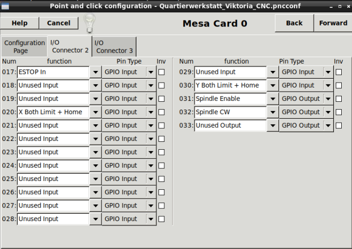
Thanks PCW! I think that I am overthinking this a bit. I will trust that the correct pins map to their correct locations. I guess the final question is with regards to the usage of PNCconf. I have basically no idea what I should fill in here:
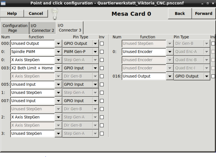
or here:
I don't understand how these map to actual db25 pins...
or here:
I don't understand how these map to actual db25 pins...
Attachments:
Please Log in or Create an account to join the conversation.
- PCW
-
- Offline
- Moderator
-
Less
More
- Posts: 17916
- Thank you received: 5245
28 Feb 2021 18:14 #200450
by PCW
Replied by PCW on topic RPI4 + 7C81 + DMB4250-8B BreakOut Board
The mapping of GPIO to DB25 pins is listed the the --readhmid output
The P3 (= 7C81 P1) mapping is correct but PNCCONF GPIO mapping on P2
(= 7C81 P2) will not line up so you probably need to do these by hand
connecting in the hal file
The P3 (= 7C81 P1) mapping is correct but PNCCONF GPIO mapping on P2
(= 7C81 P2) will not line up so you probably need to do these by hand
connecting in the hal file
Please Log in or Create an account to join the conversation.
- cmorley
- Away
- Moderator
-
Less
More
- Posts: 7316
- Thank you received: 2146
28 Feb 2021 19:02 #200455
by cmorley
Replied by cmorley on topic RPI4 + 7C81 + DMB4250-8B BreakOut Board
can you post the --readhid file?
Please Log in or Create an account to join the conversation.
- PCW
-
- Offline
- Moderator
-
Less
More
- Posts: 17916
- Thank you received: 5245
28 Feb 2021 22:39 #200475
by PCW
Replied by PCW on topic RPI4 + 7C81 + DMB4250-8B BreakOut Board
I have added DB25 pin numbers to the drivers pin list, like this:
hm2/hm2_7i95.0:     IO Pin 041 (P1-01/DB25-01): PWMGen #0, pin Out0 (PWM or Up) (Output)
hm2/hm2_7i95.0:     IO Pin 042 (P1-02/DB25-14): IOPort
hm2/hm2_7i95.0:     IO Pin 043 (P1-03/DB25-02): IOPort
hm2/hm2_7i95.0:     IO Pin 044 (P1-04/DB25-15): IOPort
hm2/hm2_7i95.0:     IO Pin 045 (P1-05/DB25-03): IOPort
hm2/hm2_7i95.0:     IO Pin 046 (P1-06/DB25-16): IOPort
hm2/hm2_7i95.0:     IO Pin 047 (P1-07/DB25-04): IOPort
hm2/hm2_7i95.0:     IO Pin 048 (P1-08/DB25-17): IOPort
hm2/hm2_7i95.0:     IO Pin 049 (P1-09/DB25-05): IOPort
hm2/hm2_7i95.0:     IO Pin 050 (P1-11/DB25-06): IOPort
hm2/hm2_7i95.0:     IO Pin 051 (P1-13/DB25-07): IOPort
hm2/hm2_7i95.0:     IO Pin 052 (P1-15/DB25-08): IOPort
hm2/hm2_7i95.0:     IO Pin 053 (P1-17/DB25-09): IOPort
hm2/hm2_7i95.0:     IO Pin 054 (P1-19/DB25-10): IOPort
hm2/hm2_7i95.0:     IO Pin 055 (P1-21/DB25-11): IOPort
hm2/hm2_7i95.0:     IO Pin 056 (P1-23/DB25-12): IOPort
hm2/hm2_7i95.0:     IO Pin 057 (P1-25/DB25-13): IOPort
Please Log in or Create an account to join the conversation.
Moderators: cmorley
Time to create page: 0.237 seconds